|
|
 |

A/D Conversion
Continuous electrical signals are converted to the digital language of computers using analog-to-digital (A/D) converters. An A/D converter may be housed on a PC board with associated circuitry or in a variety of remote or networked configurations. In addition to the converter itself, sample-and-hold circuits, an amplifier, a multiplexer, timing and synchronization circuits, and signal conditioning elements also may be on board (Figure 1-5). The logic circuits necessary to control the transfer of data to computer memory or to an internal register also are needed.
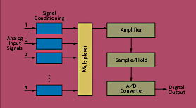 |
| Figure 1-5: Analog Input Flow Diagram |
When determining what type of A/D converter should be used in a given application, performance should be closely matched to the requirements of the analog input transducer(s) in question. Accuracy, signal frequency content, maximum signal level, and dynamic range all should be considered.
Central to the performance of an A/D converter is its resolution, often expressed in bits. An A/D converter essentially divides the analog input range into 2N bins, where N is the number of bits. In other words, resolution is a measure of the number of levels used to represent the analog input range and determines the converter's sensitivity to a change in analog input. This is not to be confused with its absolute accuracy! Amplification of the signal, or input gain, can be used to increase the apparent sensitivity if the signal's expected maximum range is less than the input range of the A/D converter. Because higher resolution A/D converters cost more, it is especially important to not buy more resolution than you need-if you have 1% accurate (1 in 100) temperature transducers, a 16-bit (1 in 65,536) A/D converter is probably more resolution than you need.
Absolute accuracy of the A/D conversion is a function of the reference voltage stability (the known voltage to which the unknown voltage is compared) as well as the comparator performance. Overall, it is of limited use to know the accuracy of the A/D converter itself. Accuracy of the system, together with associated multiplexer, amplifier, and other circuitry is typically more meaningful.
The other primary A/D converter performance parameter that must be considered is speed-throughput for a multi-channel device. Overall, system speed depends on the conversion time, acquisition time, transfer time, and the number of channels being served by the system:
Acquisition is the time needed by the front-end analog circuitry to acquire a signal. Also called aperture time, it is the time for which the converter must see the analog voltage in order to complete a conversion.
Conversion is the time needed to produce a digital value corresponding to the analog value.
Transfer is the time needed to send the digital value to the host computer's memory.
Throughput, then, equals the number of channels being served divided by the time required to do all three functions.
A/D Converter Options
While all analog-to-digital converters are classified by their resolution or number of bits, how the A/D circuitry achieves this resolution varies from device to device. There are four primary types of A/D converters used for industrial and laboratory applications-successive approximation, flash/parallel, integrating, and ramp/counting. Some are optimized for speed, others for economy, and others for a compromise among competing priorities (Figure 1-6). Industrial and lab data acquisition tasks typically require 12 to 16 bits-12 is the most common. As a rule, increasing resolution results in higher costs and slower conversion speed.
| Figure 1-6: Alternative A/D Converter Designs |
| DESIGN |
SPEED |
RESOLUTION |
NOISE IMMUNITY |
COST |
| Successive approximation |
Medium |
10-16 bits |
Poor |
Low |
| Integrating |
Slow |
12-18 bits |
Good |
Low |
| Ramp/counting |
Slow |
14-24 bits |
Good |
Medium |
| Flash/parallel |
Fast |
4-8 bits |
None |
High |
Successive approximation: The most common A/D converter design used for general industrial and laboratory applications is successive approximation (Figure 1-7). This design offers an effective compromise among resolution, speed, and cost. In this type of design, an internal digital-to-analog (D/A) converter and a single comparator-essentially a circuit that determines which of two voltages is higher-are used to narrow in on the unknown voltage by turning bits in the D/A converter on until the voltages match to within the least significant bit. Raw sampling speed for successive approximation converters is in the 50 kHz to 1 MHz range.
To achieve higher sampling speeds, a redundancy technique allows a fast initial approximate conversion, followed by a correction step that adjust the least significant bit after allowing sufficient settling time. The conversion is therefore completed faster at the expense of additional hardware. Redundancy is useful when both high speed and high resolution are desirable.
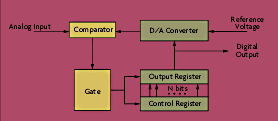 |
| Figure 1-7: A/D Conversion by Successive Approximation |
Flash/parallel: When higher speed operation is required, parallel, or flash-type A/D conversion is called for. This design uses multiple comparators in parallel to process samples at more than 100 MHz with 8 to 12-bit resolution. Conversion is accomplished by a string of comparators with appropriate references operating in parallel (Figure 1-8).
The downside of this design is the large number of relatively expensive comparators that are required-for example, a 12-bit converter requires 4,095 comparators.
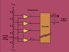 |
| Figure 1-8: A/D Conversion by Flash/Parallel Technique |
Integrating: This type of A/D converter integrates an unknown input voltage for a specific period of time, then integrates it back down to zero. This time is compared to the amount of time taken to perform a similar integration on a known reference voltage. The relative times required and the known reference voltage then yield the unknown input voltage. Integrating converters with 12 to 18-bit resolution are available, at raw sampling rates of 10-500 kHz.
Because this type of design effectively averages the input voltage over time, it also smoothes out signal noise. And, if an integration period is chosen that is a multiple of the ac line frequency, excellent common mode noise rejection is achieved. More accurate and more linear than successive approximation converters, integrating converters are a good choice for low-level voltage signals.
Ramp/counter: Similar to successive approximation designs, counting or ramp-type A/D converters use one comparator circuit and a D/A converter (Figure 1-9). This design progressively increments a digital counter and with each new count generates the corresponding analog voltage and compares it to the unknown input voltage. When agreement is indicated, the counter contains the digital equivalent of the unknown signal.
A variation on the counter method is the ramp method, which substitutes an operational amplifier or other analog ramping circuit for the D/A converter. This technique is somewhat faster.
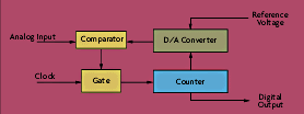 |
| Figure 1-9: A/D Conversion by Counting/Ramp Technique |
Multiplexing & Signal Conditioning
As shown in Figure 1-5, A/D converters seldom function on their own but must be considered in a systems context with associated circuitry for signal conditioning, multiplexing, amplification, and other functions. Every application will dictate a unique mix of add-ons that may be implemented in a variety of physical configurations-on a PC I/O board, inside a remote transmitter, or at a local termination panel.
Multiplexing: In many industrial and laboratory applications, multiple analog signals must be converted to digital form. And if speed is not the limiting factor, a single A/D converter often is shared among multiple input channels via a switching mechanism called a multiplexer. This is commonly done because of the relatively high cost of converters. Multiplexers also allow amplification and other signal conditioning circuitry to be time-shared among multiple channels. Software or auxiliary hardware controls the switch selection.
Sample-and-hold: It is important to acknowledge that a multiplexer does reduce the frequency with which data points are acquired, and that the Nyquist sample-rate criterion still must be observed. During a typical data acquisition process, individual channels are read in turn sequentially. This is called standard, or distributed, sampling. A reading of all channels is called a scan. Because each channel is acquired and converted at a slightly different time, however, a skew in sample time is created between data points (Figure 1-10).
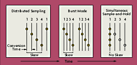 |
Figure 1-10: Alternative Methods for Eliminating
Time Skew Among Multiplexed Channels |
If time synchronization among inputs is important, some data acquisition cards offer �burst� mode operation or simultaneous �sample-and-hold� circuitry. Burst mode, or pseudo-simultaneous sampling, acquires each channel at the maximum rate of the board, then waits a user-specified amount of time before sampling again.
True simultaneous sample-and-hold systems can sample all channels within a few nanoseconds of each other, eliminating phase and time discontinuities for all but the fastest processes. Essentially, a switched capacitor on each channel tracks the corresponding input signal. Before starting the A/D conversion process, all switches are opened simultaneously, leaving the last instantaneous values on the capacitors.
Signal scaling: Because A/D converters work best on signals in the 1-10 V range, low voltage signals may need to be amplified before conversion-either individually or after multiplexing on a shared circuit. Conversely, high voltage signals may need to be attenuated.
Amplifiers also can boost an A/D converter's resolution of low-level signals. For example, a 12-bit A/D converter with a gain of 4 can digitize a signal with the same resolution as a 14-bit converter with a gain of 1. It's important to note, however, that fixed-gain amplifiers, which essentially multiply all signals proportionately, increase sensitivity to low voltage signals but do not extend the converter's dynamic range.
Programmable gain amplifiers (PGAs), on the other hand, can be configured to automatically increase the gain as the signal level drops, effectively increasing the system's dynamic range. A PGA with three gain levels set three orders of magnitude apart can make a 12-bit converter behave more like an 18-bit converter. This function does, however, slow down the sample rate.
From a systems perspective, amplifier performance should be on par with that of the A/D converter itself-gain accuracy should be specified as a low percentage of the total gain. Amplifier noise and offset error also should be low.
Other conditioning functions: Other A/D signal conditioning functions required will vary widely from application to application. Among the options:
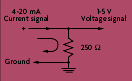 |
Figure 1-11: Conversion
of 4-20 mA to 1-5 V |
Current-to-voltage conversion: A 4-20 mA current signal can be readily converted to a voltage signal using a simple resistor (Figure 1-11). A resistor value of 250 ohms will yield a 1-5 V output.
Filtering: A variety of physical devices and circuits are available to help separate desired signals from specific frequencies of undesirable electrical noise such as ac line pick-up and other electromagnetic/radio frequency interference (EMI/RFI). If the signal of interest is lower in frequency than the noise, a low-pass filter can be used. High-pass and notch-band filters are designed to target low frequency interference and specific frequency bands, respectively.
Excitation: Voltage supplied by the data acquisition card or discrete signal conditioner to certain types of transducers such as strain gages.
Isolation: Used to protect personnel and equipment from high voltages. Isolators block circuit overloads while simultaneously passing the signal of interest.
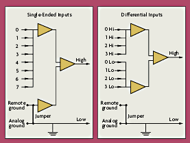 |
Figure 1-12: Single-ended & Differential
Analog Input configurations |
Single-Ended & Differential Inputs
Another important consideration when specifying analog data acquisition hardware is whether to use single-ended or differential inputs (Figure 1-12). In short, single-ended inputs are less expensive but can be problematic if differences in ground potential exist.
In a single-ended configuration, the signal sources and the input to the amplifier are referenced to ground. This is adequate for high level signals when the difference in ground potential is relatively small. A difference in ground potentials, however, will create an error-causing current flow through the ground conductor otherwise known as a ground loop.
Differential inputs, in contrast, connect both the positive and negative inputs of the amplifier to both ends of the actual signal source. Any ground-loop induced voltage appears in both ends and is rejected as a common-mode noise. The downside of differential connections is that they are essentially twice as expensive as single-ended inputs; an eight-channel analog input board can handle only four differential inputs.
|